Superconducting detectors & quantum sensors
I-V characteristics, critical current and response testing of SNSPDs, SQUIDs, TESs and other superconducting devices.

Build a cryogenic test environment around sample temperature, heat load and measurement interfaces, combining a cryostat, temperature control and experimental accessories.
Twelve typical research directions across four fields: superconducting electronics, cryogenic electronics & quantum technology, cryogenic optics & optoelectronics, and materials & multi-field physics. Each has different needs for temperature range, cooling power, stability, vibration and optical / electrical / RF access — use them to plan a cryogenic test platform.
I-V characteristics, critical current and response testing of SNSPDs, SQUIDs, TESs and other superconducting devices.
Testing superconducting filters, resonators, mixers and oscillators with low-loss RF wiring from DC to 40 GHz.
Cryogenic electrical characterization and noise testing of Josephson junctions and SQUID loops.
Characterization and model-parameter extraction for cryo-CMOS, cryogenic amplifiers and quantum readout circuits.
Screening, wiring verification and basic electrical tests of superconducting and semiconductor quantum devices before ultra-low-temperature runs.
Calibration and comparison of silicon-diode thermometers, resistance thermometers and other cryogenic sensors.
Optoelectronic characteristics and efficiency of LEDs, laser diodes and photodetectors at low temperature.
Temperature-dependent PL and Raman of quantum dots, color centers and 2D materials, with cryogenic objectives and piezo stages.
Response, noise and dark current of IR detectors, focal-plane arrays and optoelectronic chips at operating temperature.
Resistance–temperature, critical-temperature and magnetotransport measurements of phase transitions in superconducting and correlated-electron materials.
Properties of 2D and emerging materials under coupled mechanical, thermal, optical, electrical and magnetic fields.
Thermal conductivity, thermal expansion and heat-load assessment of cryogenic components for cryogenic systems and space payloads.
Cryogen-free closed-cycle cooling and vacuum chambers provide a stable low-temperature environment.
Sample stages, optical windows / fibers and DC–RF wiring bring in samples and signals.
Multi-channel thermometry and PID control hold set points and run temperature sweeps.
Connect electrical, optical or RF instruments for transport, spectroscopy and device characterization.
An indicative experimental workflow. Modules and compatibility are confirmed for each configuration.
Select temperature range, cooling power and sample space.
Choose signal and optical accessories for the measurement chain.
Configure vacuum accessories around pumping and signal connections.
One-stop optical, electrical and quantum-materials test solutions from room temperature down to cryogenic temperatures, for research and industry.
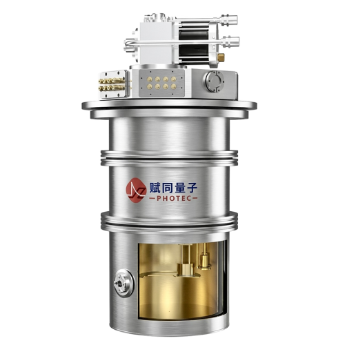 Helium Matrix-1K / 0.3K | 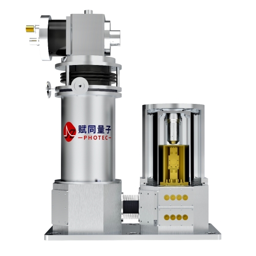 Helium Matrix-4K | 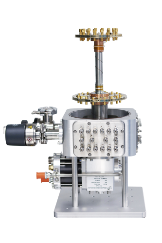 Helium Matrix-4K | |
|---|---|---|---|
| Type | Sub-kelvin cryostat | Cryogenic optical cryostat | Cryogenic optical cryostat |
| Minimum temperature | 850 mK / 300 mK | 2–4.2 K | 2–4.2 K |
| Cooler | GM / adsorption | GM | GM |
| Cooling power | 100 μW at 850 mK 50 μW at 350 mK | 0.1–1 W at 4.2 K | 0.1–1 W at 4.2 K |
| Temperature stability | ±25 mK | ±5 to ±50 mK | ±5 to ±50 mK |
| 24/7 operation | |||
| Low-vibration option | — | — |
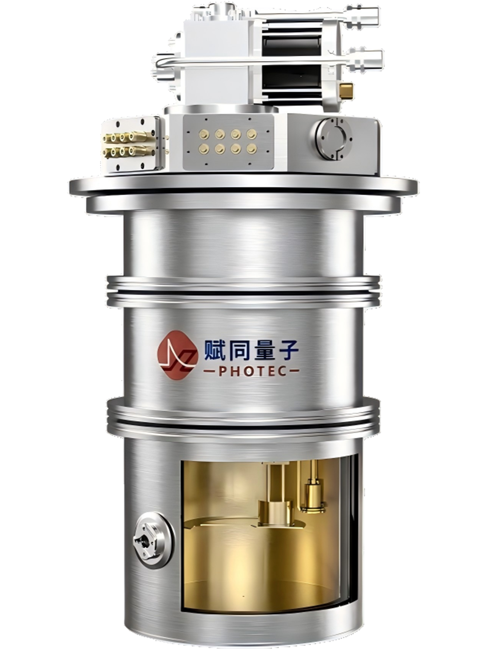
0.3–300 K without liquid helium; low vibration, high stability, easy maintenance
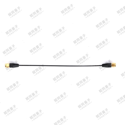
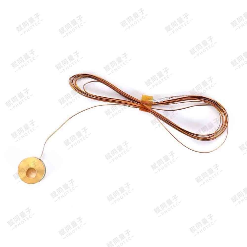
Signal interconnects across temperature stages; standard connectors, low heat leak, crosstalk and loss
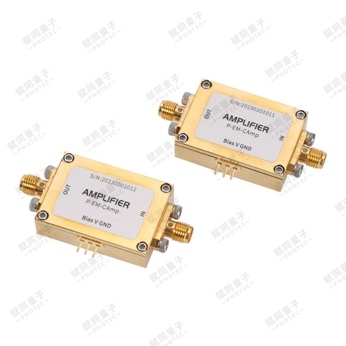
Amplify signals cold to suppress thermal noise and improve SNR; low loss, EMI resistant
Open, modular architecture for coupled mechanical, thermal, optical, electrical and magnetic experiments
 Cryogenic piezo stages
 Cryogenic objectives
 Electrical probe stage
 DC / RF interfaces
 Optical windows / fibers
 Chamber & sample-stage extensions
SQUID and SNSPD characterization; superconducting filters, mixers and oscillators
Case studiesCryogenic optoelectronic devices and chips: LEDs, laser diodes, photodetectors
Case studiesCryo-CMOS and cryogenic semiconductor sensors
Case studiesMulti-field properties of 2D and superconducting materials
Case studiesShare your sample, measurement goals and existing equipment so we can discuss a suitable configuration.